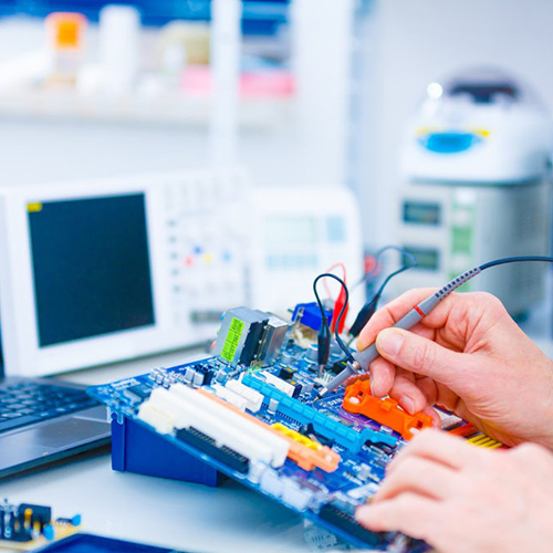
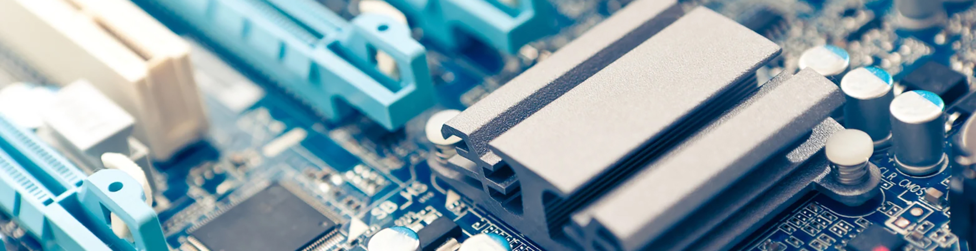
The transition to sub-5nm and 3nm technology nodes has pushed semiconductor manufacturing into an era where physical and chemical tolerances are practically nonexistent. In modern fabrication facilities (fabs), equipment uptime, process yield, and contamination control dictate profitability. Even microscopic particulate generation or a micro-millimeter of thermal expansion can ruin an entire wafer, costing hundreds of thousands of dollars. To address these extreme operational demands, equipment manufacturers have systematically replaced traditional metals and alloys with advanced technical ceramics.
Components within etching chambers, chemical vapor deposition (CVD) systems, and ion implantation machines face some of the most hostile environments in any industry. They are subjected to aggressive halogen plasmas, extreme thermal cycling, and continuous mechanical stress. Understanding how specific ceramic materials behave under these conditions is essential for engineering reliable, high-yield manufacturing systems.
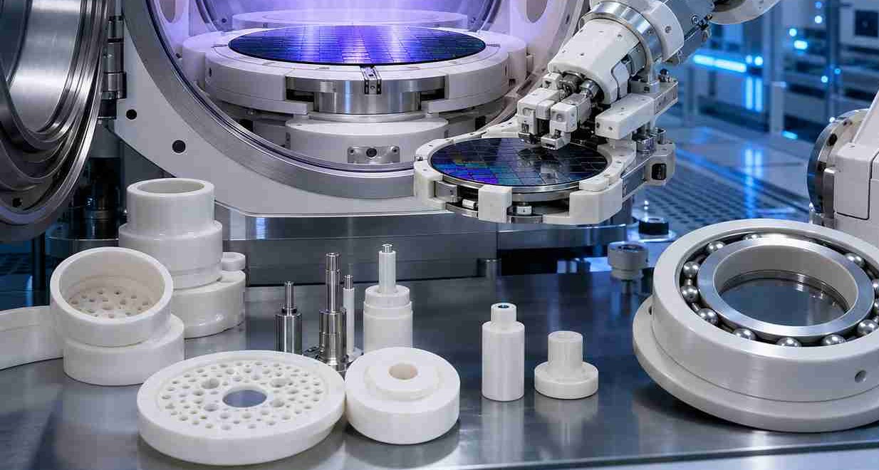
Plasma-enhanced processes, particularly reactive ion etching (RIE), rely on highly volatile gases like fluorine, chlorine, and bromine. When ignited into a plasma state, these gases actively strip away material from the silicon wafer. Unfortunately, they also attack the internal components of the process chamber. When traditional metals like anodized aluminum are exposed to these plasmas, they degrade, flaking off metallic contaminants that settle on the wafer surface, causing immediate yield loss.
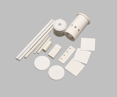
To solve this, chamber liners, gas distribution plates, and focus rings require materials with extreme chemical inertness. This is where 99% Alumina Ceramic Semiconductor Components become highly effective. High-purity alumina (Al₂O₃) demonstrates exceptional resistance to fluorine-based chemistries. Because it is practically free of impurities like silica or iron oxide, it does not form volatile byproducts when bombarded by plasma ions. This structural integrity prevents the generation of microscopic particles, significantly extending the mean time between cleans (MTBC) for the processing chamber.
| Material | Plasma Resistance (Fluorine) | Contamination Risk | Typical Application |
|---|---|---|---|
| Anodized Aluminum | Low | High (Metallic flaking) | Low-stress structural parts |
| Quartz | Moderate | Medium (Oxygen release) | Viewports, specific etch processes |
| 99% Alumina Ceramic | High | Extremely Low | Chamber liners, Gas showerheads |
Semiconductor manufacturing involves rapid and extreme temperature fluctuations. Thermal processing steps, such as rapid thermal annealing (RTA) or epitaxial growth, can push chamber temperatures above 1000°C in a matter of seconds. Components must possess a low coefficient of thermal expansion (CTE) to prevent warping, cracking, or shifting out of alignment. If a wafer handling arm expands even slightly, the wafer may be placed off-center, leading to uneven deposition or structural damage.
Integrating Precision Ceramic Parts For Semiconductor Equipment is the standard engineering response to thermal variability. Advanced ceramics can be machined to exacting tolerances—often within a few microns—and they hold these dimensions regardless of thermal shock. For instance, electrostatic chucks (ESCs), which hold the silicon wafer in place during processing, rely on precisely machined ceramic layers. The ceramic material must match the thermal expansion rate of the silicon wafer as closely as possible to prevent mechanical stress on the wafer itself. The excellent thermal conductivity of specialized ceramics also ensures uniform heat distribution across the wafer, directly influencing the consistency of the integrated circuits being formed.
| Property | Silicon (Wafer) | Aluminum Alloy | Precision Ceramic (Alumina/AlN) |
|---|---|---|---|
| Coefficient of Thermal Expansion (10⁻⁶/K) | ~ 2.6 | ~ 23.0 | ~ 4.5 to 8.0 |
| Maximum Operating Temperature | - | 400°C | 1400°C - 1600°C |
| Dielectric Strength (kV/mm) | - | N/A (Conductor) | > 15 |
A fab operates 24 hours a day, 7 days a week. The automated material handling systems, vacuum load locks, and robotic end-effectors are in continuous motion, moving silicon wafers from one processing module to the next. Frictional wear in these mechanical parts generates microscopic dust. In a Class 1 cleanroom environment, dust generation is unacceptable. Furthermore, component degradation leads to mechanical failure, triggering unscheduled downtime.
Standard ceramics can sometimes be brittle, making them susceptible to chipping upon impact. However, transformation-toughened materials solve this problem. Deploying Zirconia Ceramic Components For Industrial Equipment provides a massive upgrade in fracture toughness. Zirconia undergoes a phase transformation when placed under mechanical stress, which effectively stops crack propagation in its tracks. This unique property makes zirconia ideal for moving parts, such as ceramic bearings, guide pins, and robotic arm linkages. It provides the hardness and wear resistance characteristic of ceramics while offering the durability needed to withstand continuous mechanical shock and vibration without shedding particulate matter.
Beyond mechanical and thermal properties, the electrical characteristics of components play a heavy role in equipment reliability. Many semiconductor processes rely on strong electromagnetic fields to control plasma density and directionality. Components placed near these fields must be highly insulative to prevent electrical arcing, which can instantly destroy a wafer and damage surrounding hardware.
High-purity ceramics act as excellent electrical insulators at both high voltages and high frequencies. They boast high dielectric strength and low dielectric loss. In radio frequency (RF) driven plasma chambers, ceramic isolation rings and structural standoffs prevent power leakage and maintain the stability of the RF field. This electrical stability directly correlates to the uniformity of the etching or deposition process happening on the wafer surface. A fluctuation in the electrical field, caused by a poorly insulated component, will result in uneven microchip features across the wafer, reducing the overall yield of usable processors.
| Equipment Component | Primary Challenge | Optimal Ceramic Solution | Resulting Benefit |
|---|---|---|---|
| Electrostatic Chuck (ESC) | Thermal distribution, electrical hold | Precision Machined Alumina/AlN | Zero wafer warpage, uniform processing |
| Robotic End-Effectors | Friction, vibration, particulate generation | Toughened Zirconia | Extended lifespan, zero particle shedding |
| Plasma Chamber Liners | Halogen corrosion, ion bombardment | 99%+ Purity Alumina | Longer MTBC, high wafer yield |
The justification for using highly engineered ceramics comes down to the metric of Overall Equipment Effectiveness (OEE) and Mean Time Between Failures (MTBF). A modern extreme ultraviolet (EUV) lithography system or high-density plasma etcher represents an investment of tens to hundreds of millions of dollars. Unplanned downtime for such equipment is calculated in thousands of dollars per minute. Every time a chamber must be vented to atmospheric pressure to replace a degraded metal component, the fab loses hours of production time due to the requisite cooling, part replacement, pump-down, and recalibration phases.
By integrating advanced ceramics, equipment engineers extend the maintenance intervals drastically. A component that might need replacement every 30 days when made from standard metals can often operate continuously for 6 to 12 months when fabricated from high-purity alumina or wear-resistant zirconia. This multiplication of equipment uptime amortizes the higher initial cost of ceramic parts rapidly. Furthermore, the reduction in wafer scrap due to particulate contamination provides an immediate financial return.
The trajectory of semiconductor manufacturing demands continual reduction in defect rates alongside higher process temperatures and more aggressive chemistries. As the industry advances further into gate-all-around (GAA) transistors and advanced 3D packaging, the operational parameters of manufacturing equipment will become even stricter. Material science remains the foundational layer that makes these architectural leaps possible, relying heavily on the predictable, stable, and highly resilient properties of engineered technical ceramics to keep fabrication lines running smoothly.

24/7 Call Service +8618018373518
Email : yxshenxing88@vip.163.com
Address : No. 2022, Baoyang Road, Chuanbu Industrial Zone, Yixing City, Wuxi City, Jiangsu Province


 2025-10-14
 2025-10-14
blog Xml Privacy Policy Sitemap
Copyright @ 2026 Yixing Shenxing Technology Co., Ltd. All Rights Reserved.
 Network Supported
leave a message
Scan to wechat :

Scan to whatsapp :